This topic contains a solution. Click here to go to the answer
|
|
|

 Nitrogen fluxes in Sycamore Creek, Arizona (data from Grimm 1988).
 Demonstrate the Application of Triangular, Figure-Eight, and Tubular Bandages
 Demonstrate the Application of Triangular, Figure-Eight, and Tubular Bandages
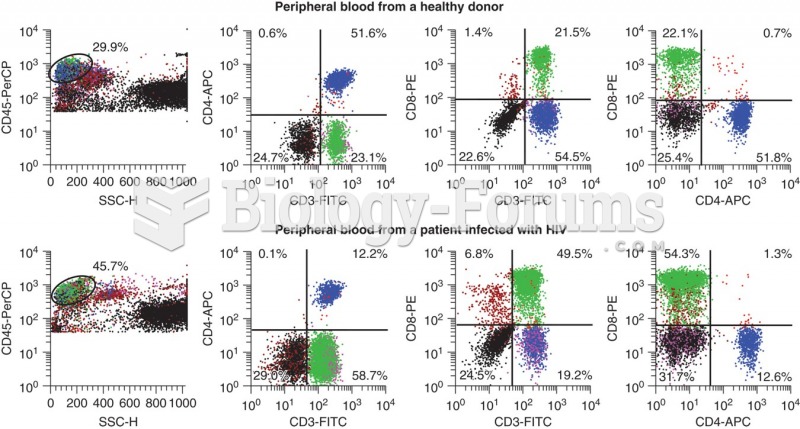 Flow data for a healthy donor (top panel) and a HIV positive patient. CD3 is a T-cell marker, CD4 is ...
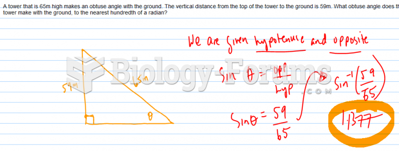 Application Special Triangles
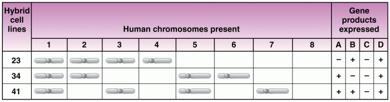 A hypothetical grid of data used in synteny testing