This topic contains a solution. Click here to go to the answer
|
|
|

 Electronic service information is available from aftermarket sources, such as All-Data and ...
 Acquiring Weather Data
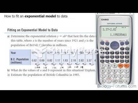 How to fit an exponential model to data
 How to solve application problems containing quadratics (Question 1)
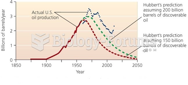 Hubbard’s Predication of Peak in U.S Oil Production with Actual Data
 Application and Integration