This topic contains a solution. Click here to go to the answer
|
|
|

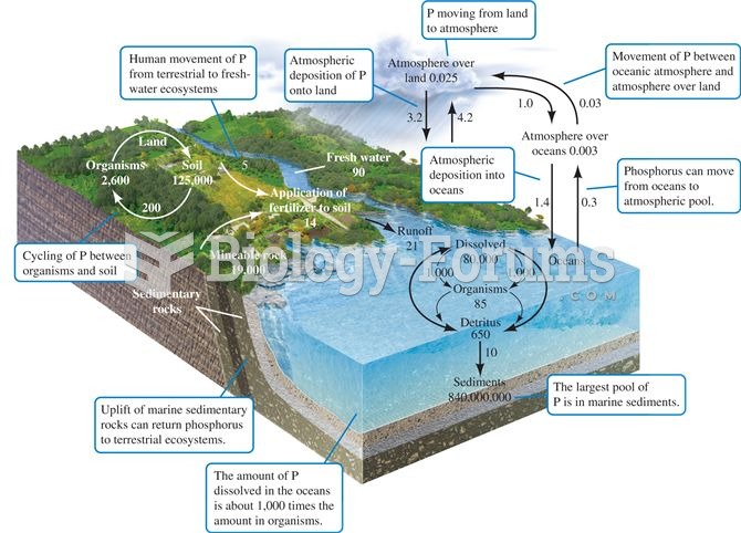 The phosphorus cycle. Numbers are 1012 g P or fluxes as 1012 g P per year (data from Schlesinger 199
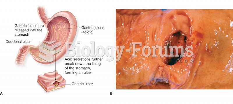 (A) Figure illustrating the location and appearance of a peptic ulcer in both the stomach and the du
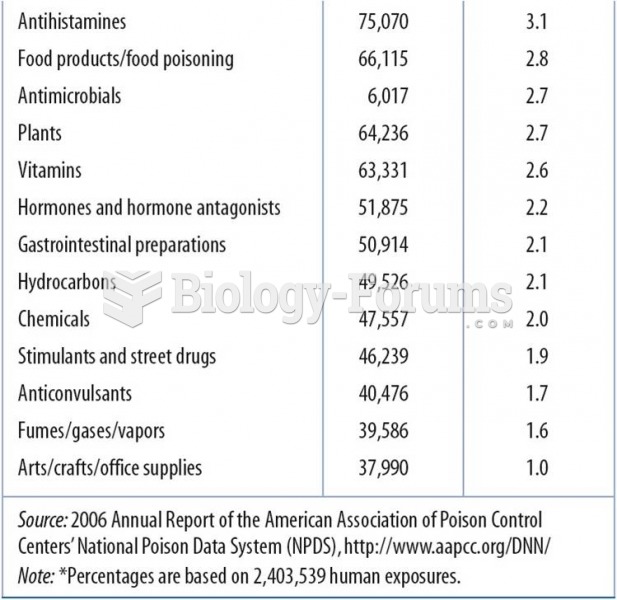 2006 Data:Top 25 Substances Involved in Human Exposures
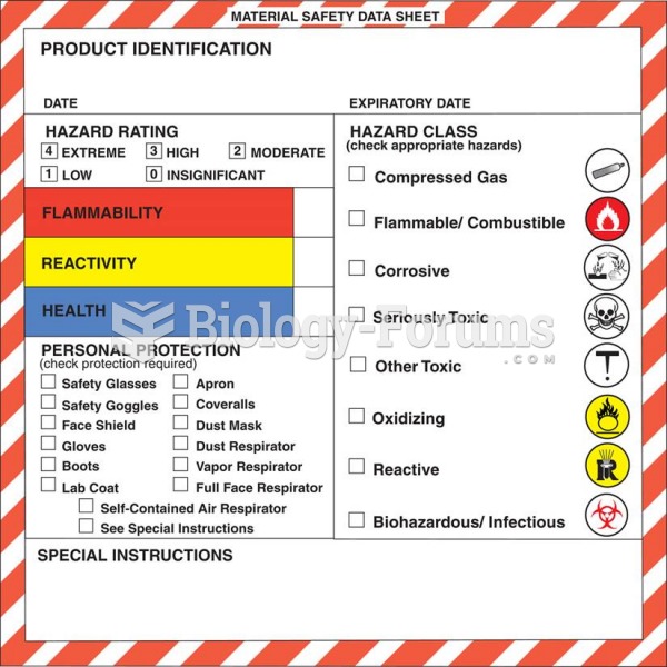 An example of a Material Safety Data Sheet (MSDS).
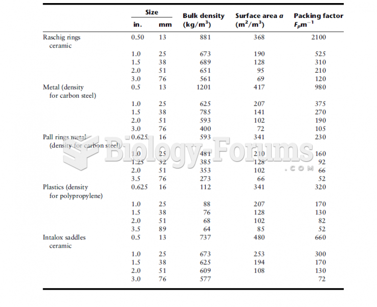 Design Data for Various Packings
 How to solve application problems containing quadratics (Question 3)